| WASEDA UNIVERSITY |
|
|
|
||
|
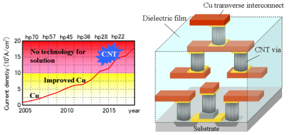
A large scale integration (LSI) used in the electric equipments such as a computer and a mobile phone has realized high performance with scaling down its size. However, international technology roadmap for semiconductors (ITRS) 2005 reported that the current density required for wiring materials will exceed that of Cu (107 A/cm2) by 2014 as shown in Fig. 1(a), and the increasing bulk resistance of Cu by electron scattering becomes a serious problem with miniaturization of Cu wiring. Carbon nanotubes (CNTs) are promising materials for future LSI interconnects because of their unique properties: high current density exceeding 109 A/cm2, high thermal conductivity, and ballistic transport. For multilayer interconnect applications, it is essential to synthesize CNT bundles at temperatures below 400°C to reduce the damage to the interlayer dielectric film. Moreover, lowering the resistance of interconnects can reduce the RC wiring delay and improve the speed of processing. Although the resistance of one CNT is inferior to that of Cu, the resistance of CNT can exceed Cu by forming dense bundles. Therefore, the density of CNT is very important for wiring application. The purpose of this study is replacing the via interconnects by dense CNT bundles grown below 400°C as shown in Fig. 1(b). |
||
Fig. 1 (a) The requirement of current density tolerance for future ULSI (by ITRS2005). |
||
|
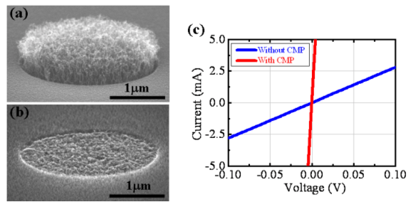
We fabricated the circuit using CNT vias and Cu as shown in Fig. 1(b) and succeeded in measuring the performance of CNT as interconnects. This structure had the vertical interconnects consisted of CNT vias and the Cu transverse interconnects. The CNTs were synthesized with remote plasma chemical vapor deposition (RP-CVD) and Co catalyst particles at 390℃. Figure 2(a) shows the CNTs grown from the via hole and Fig. 2(b) shows the CNTs whose surface area was planarized by chemical mechanical polishing (CMP). The CMP has already been used in the Si LSI process to planarize the Cu interconnects. The measured resistances of CNT vias are shown in Fig. 2(c). The resistance of CNTs with CMP was superior to that of CNTs without CMP. This demonstrated that the CNTs grown at the low temperature which meets the requirement of LSI process could act as the carrier path. Although the resistance of CNTs was higher than that of Cu, the value was top level in the world. From now on, we aim at increasing the CNT density by optimization of CVD condition to reduce the resistance. |
||
Fig. 2
(a) CNTs grown from via structure |
||
Acknowledgement This work was completed as part of the MIRAI Project supported by NEDO. Refecence [1] D. Yokoyama, T. Yoshida, T. Iwasaki, S. Sato, T. Hyakushima, M. Nihei, Y. Awano, H. Kawarada "Low temperature grown carbon nanotube interconnects using inner shells by chemical mechanical polishing", Appl. Phys. Lett., 91, 26, 263101 (2007) |
||