| WASEDA UNIVERSITY |
|
|
|
||
|
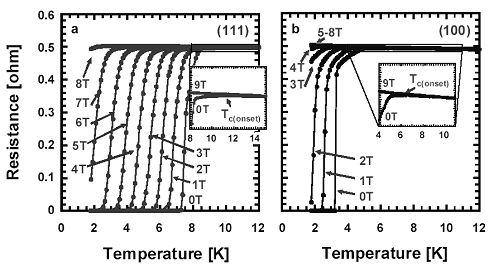
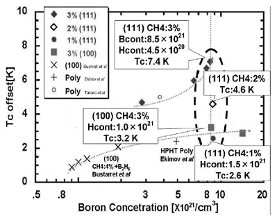
Boron doping on diamond Diamond is an electrical insulator with a wide band gap of 5.5 eV, well known for its hardness as well as its exceptional electronic and thermal properties. Semi conducting diamond can be obtained by introducing impurity atom to diamond lattice which contain carbon, an element of the fourth group of the periodic table, with the same crystal structure as silicon. Each carbon atom has four near neighbors with which it forms covalent bonds in a tetrahedral configuration. Introducing impurity atom of the third or fifth group of the periodic table could form acceptor or donor impurity level and contribute carriers which can be activated just as that of silicon. Because of its small atomic radius compared to other potential dopants, boron is readily incorporated into the dense (1.763×10²³ atoms cm-3) diamond lattice with high reproducibility and high enough concentration to be useful for electronic devices. Doped diamond exhibit impurity level of 0.37 [eV][1] for boron, too high to be activated at room temperature. Boron can be incorporated into diamond lattice by high temperature high pressure synthesize (HPHT) or chemical vapor deposition (CVD). Superconductivity on boron doped diamond Discovery of Type-II superconductivity was on polycrystalline diamond synthesized at pressure (8-9 GPa) and temperature (2500-2800 K). This discovery by Ekimov et al [3], with Tc=4K, revived the question of mechanisms in strongly covalent materials. We used chemical vapor deposition method, which is widely used for the synthesis of high quality layers for electronic applications. Boron concentration incorporated in diamond lattice can be controlled by this method, making it possible to investigate change of conductivity as boron concentration increase on diamond. We have recorded highest Tc observed on diamond Tc=7.4K for (111) and Tc=3.2K for (100). An alternative theoretical approach [4] stresses out the fact that the boron concentration range where superconductivity has been observed is close to the Anderson-Mott Metal-Insulator Transition [5] and suggests an electron correlation driven extended s-wave superconductivity in the boron impurity band. A degenerate semiconductor with superconducting properties can be used as way to investigating electron-electron and electron-phonon interactions in both the normal and the superconducting states. A semiconductor of this type could also be used to give further information about the band structure of semiconductors. Further, in the case of the carbon clathrates, it has been predicted that the electron-phonon potential Vep=λ/N(EF) may be extremely large. Boron doped diamond is a promising material for exploring hetero-conduction structure and what happens at boundary of this hetero-conduction structure is still to be investigated. And new device structure can be thought using different conducting states as a tool to amplify carriers. Boron doped diamond by microwave assisted CVD system We have grown homoepitaxial boron doped diamond on (100), (111) Ib diamond substrate using microwave assisted CVD. Conditions for diamond growth were 60-80 Torr chamber pressure, 600 W micro wave power, 800-900℃ substrate temperature with diluted gas mixtures of methane and trimethylboron (TMB) in hydrogen. The methane concentration is 0-3% in hydrogen with a B/C ratio of 0-12000 ppm. Films of 1-4μm thickness were used for the following measurements. Superconductivity has been observed by transport and the magnetization properties measurement using a superconducting quantum interference device (SQUID) magnetometer and by resistivity measurement using Van der Pauw theory and Particle Property Measurement System (PPMS). Boron concentration for thin films were measured by secondary ion mass spectroscopy (SIMS) measurement, ranging from 2.8×10¹⁹〜1.4×10²²[cm-3]. Boron concentration and Tc The temperature dependences of the resistivity are measured on the (100) and (111) diamond films. The resistance characteristics of the (111) and (100) diamond films under the zero field condition as a function of temperature are shown in Figure 1. From Figure 1 Tc(onset) and Tc(offset) obtained for (111) diamond is 11.4 K and 7.4 K, respectively. On the other hand, Tc(onset) and Tc(offset) for (100) diamond film are 6.3 K and 3.2 K, respectively, they are twice as low as those of the (111) film. Figure 2 shows the experimental results of Tc(onset) and Tc(offset) for heavily boron doped diamond (111) and (100), and polycrystalline diamond, as well as those reported in [3], [6] and [7] as functions of boron concentration. The Tc(onset) and Tc(offset) of (111) diamond films increase without saturation up to 8×1021 cm-3 (4.5%). On the other hand the Tc of (100) films seems to saturate at 8.5 × 1021 cm-3 with the Tc(offset) of 3.2 K in (100) diamond. A slightly lower Tc(offset) of 2.9 K is obtained in (100) diamond with a higher boron content (1.4×1022 cm-3, 7.9%), which is the highest boron concentration ever reported on diamond. |
||
|
Figure 1. RT measurement of (111) and (100) diamond films with Nb=8.4 x 1021cm-3 |
||
|
Figure 2. Tc vs Boron Concentration |
||
|
Conclusions The band structure of a semiconductor can be changed for a given band structure by changing the doping. The carrier concentration and band structure of a degenerate semiconductor can therefore be varied independently of one another and, the superconductivity could then be observed as a function of band-structure changes and changes in the number of carriers alone. Band dispersion of boron doped diamond has been measured by ARPES [8] and observed results show same band structure for changing boron concentration. However, Fermi Level of diamond lowers as boron concentration increase. From these results it can be concluded that diamond is acting as carrier sink with constant band structure where electron-phonon interaction can occur. Reason for difference between (100) and (111) facets has not been explained, as mechanism of superconductivity on B-doped diamond has not been well understood. It could be change of band structure for different effective mass of holes that exist in degenerate state. It is believed that change of lattice constant is responsible for change of band dispersion for each hole, making it easier for copper pairs to form, thus leading to a superconductive state. Reference [1] K. Thonke, Semicond. Sci. Technol. 18, S20 (2003). |
||