| |
|
|
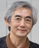
 PROFESSOR: PROFESSOR:
川原田 洋, Hiroshi Kawarada, Dr


| 1978 |
|
Bachelor of Engineering, School of Science and Engineering, Waseda University.
1980,Master of Engineering, Graduate School of Science and Engineering,
Waseda University. |
| 1980-1982 |
|
Semiconductor & Integrated Circuits Division, Hitachi Ltd. |
| 1985 |
|
Doctor of Engineering, Graduate School of Science and Engineering,
Waseda University. |
| 1986-1990 |
|
Assistant Professor, Faculty of Engineering, Osaka University. |
| 1990-1995 |
|
Associate Professor, School of Science and Engineering, Waseda University. |
| 1995- |
|
present, Professor, School of Science and Engineering, Waseda University. |
| 2009-2010 |
|
Director, Research Organization for Nano-science & Nano-technology |
| 2010- |
|
Member, Kagami Memorial Research Institute for Materials Science and Technology |
| 1998-2008 |
|
Organizer, European Conference on Diamond, Carbon Nanotube, and Related Materials. |
| 2005-2007 |
|
Board Member, Japan Applied Physics Society |
| 2009-2014 |
|
Chairman, New Diamond Forum |
| 2012- |
|
Member, Science Council of Japan |
| 2016 |
|
The Commendation for Science and Technology by the Minister of Education, Culture, Sports, Science and Technology, Research Category |
| 2017- |
|
Visiting Professor, Institute of Materials and Systems for Sustainability, Nagoya University |
| 1995-1996 |
|
Research Fellowship, Alexander von Humboldt Foundation
Fraunhofer Institute for Applied Solid State Physics |
| 1998-2003 |
|
Leader: CREST Project (JST) "Fine structured Diamond Electron Devices Formed by Controlling Surface Adsorbates" |
| 2003-2005 |
|
Leader: Grant in Aid for Scientific Research (A) “Development of High Frequency and High Power Transistors by Controlling Diamond Surface Conductivity ”
2007-2011 Team Leader Grant in Aid for Scientific Research (S) “Development of High Power and Millimeter-long Wave Diamond Transistors Using Two Dimensional Hole Gas” |
| 2010- |
|
Leader: Low-Carbon Research Network Japan (Lcnet) “Center for Ultra-Low-Loss Power Diamond Transistor” |
| 2011-2013 |
|
Leader: Grant in Aid for Scientific Research (A) “High Sensitivity Protein Chip by Aptamer Immobilized Diamond Surface” |
| 2011-2015 |
|
Leader: Advanced Low Carbon Technology Research & Development Program (ALCA) “Basic Technologies For Green Inverter Using Large Diameter Diamond Substrates” |
| 2014-2018 |
|
Leader: Grant in Aid for Scientific Research (S) “Electron Spin Control of Diamond by Surface Carrier and its Application to Nuclear Spin Detection of Bio-Molecules” |
| 2022-2024 |
|
Leader: Grant-in-Aid for Challenging Exploratory Research
“Marine communication based on a new principle using longitudinal waves generated by polarization in a liquid electrolyte” |
| 2024-2026 |
|
Leader: Grant in Aid for Scientific Research (B)
“P-channel Diamond Field Effect Transistors For Complementary High-speed Power Inverters” |
|
|

