| WASEDA UNIVERSITY |
|
|
|
|||||||||
|
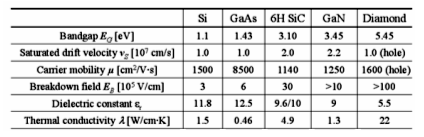
1. Why diamond is expected for future RF devices? The third generation or newer mobile communication systems require high-power and low-distortion power amplifiers based on the development of extremely high power RF transistors. Recently, diamond has attracted attention as a material for high-power and high frequency devices due to its superior material properties such as a wide band gap (5.45eV), a high breakdown field (10MV/cm), a high thermal conductivity (22W/cmK) and a small dielectric constant (5.7). Material properties of semiconductors including diamond are shown in table 1. However, because of the high activation energy of impurities in diamond, the performance of diamond transistors with conventional doping (boron) is much lower than the expected values, especially at room temperature. |
|||||||||
|
Table. 1 Material properties of semiconductors
|
|||||||||
|
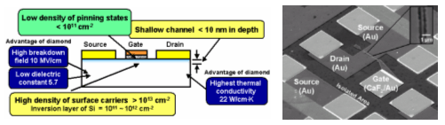
The surfaces of diamond films deposited by MPCVD (microwave plasma assisted chemical vapor deposition) are terminated by hydrogen atoms. The hydrogen-terminated (H-terminated) diamond surface generates 2-dimensional hole accumulation layer without impurity doping such as boron. This hole accumulation layer is suitable for use as the channel of field-effect transistors (FETs) because of the following excellent properties. The sheet carrier density of the holes is as high as 1013/cm2. The carriers are confined in a shallow subsurface region of less than 10nm thickness. The H-terminated surface exhibits a low density of surface states, less than 1011/cm2. Consequently, FETs utilizing H-terminated surface channel show better characteristics than impurity doped diamond devices [1][2]. The device structure and SEM picture are shown in fig 2. |
|||||||||
|
Fig. 2 Structure of diamond devices |
|||||||||
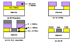
2. How to make diamond MISFETs. RF diamond MISFETs were fabricated on as-grown homoepitaxial diamond films deposited on HPHT (high-pressure-high-temperature synthetic) type Ib (001) diamond substrates by MPCVD. Sheet resistance, hole mobility and sheet carrier concentration values are <10kΩ/sq, 50-100cm2/Vs and ~1013cm-2, respectively. Au for source and drain electrodes is deposited on diamond surface. The gate was fabricated by self-align process. The process flow is shown in fig 3. |
|||||||||
Fig. 3 Process flow of diamond MISFETs |
|||||||||
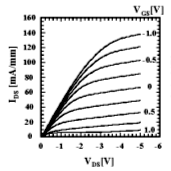
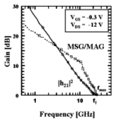
3. ACHIEVED RESULTS!! Fig 4 shows the typical DC characteristic of 0.2μm gate MISFET. The maximum saturated drain-source current (Ids) and the maximum transconductance is 140mA/mm and 48mS/mm, respectively for 50μm gate-width. |
|||||||||
|
|||||||||
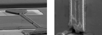
~Diamond MISFETs with T-shaped gate~ The gate length miniaturization improves fT, but improvement of fmax is not as high as that of fT because of gate resistance (Rg) increase. So, we fabricated MISFETs with a gate length of 0.2μm and a T-shaped gate structure. The T-shaped gate structure decreases Rg because T-shaped gate structure has a lager cross-section area than normal gate structure. The SEM picture of the device is shown in fig 6. |
|||||||||
Fig. 6 T-shaped gate of a diamond MISFET |
|||||||||
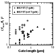
| The Rg was decreased to 5Ω by applying for the T-shaped gate structure. Consequently the fmax/fT ratios are increased markedly for diamond MISFETs. The (fmax/fT)2 value is 4, which is large for submicron-gate diamond MISFETs (Fig. 7)[4]. | |||||||||
Fig. 7 fmax/fT ratio VS gate length |
|||||||||
~Diamond MISFETs with Al2O3 gate insulator~ Generally, in application to semiconductor devices, including diamond FETs, fabrication of the gate insulator is a key technology to achieve high performance and ensure reliability, such as low gate leakage current. In particular, fabrication of the gate insulator-diamond interface is one of the most important processes for diamond MISFETs to extract the high potential of diamond, such as high breakdown voltage. Therefore, a gate insulator with high breakdown voltage, high dielectric constant, and a stable structure is desirable. Aluminum oxide is a well characterized gate insulator material to reduce gate leakage current for ULSI devices because aluminum oxide has a wide band gap, high dielectric constant, and high breakdown voltage. So, using PLD (Pulsed Laser Deposition) process to deposit Al2O3, we fabricated successfully diamond MISFETs with aluminum gate insulator of 25nm[5]. |
|||||||||
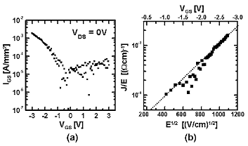
Fig.8 Gate leakage characteristic of MISFETs with Al2O3 gate insulator (Gate length = 1.5 um). |
|||||||||
4. References [1] H. Kawarada, M. Aoki, M. Ito, "Enhancement mode metal-semiconductor field effect transistors using homoepitaxial diamonds", Appl. Phys. Lett. 65, 1563 (1994) |
|||||||||